Layer:
1-32Material:
Fr-4PCB Thickness:
0.8mmCu Thickness:
1.5 OZMin line W/S:
0.1/0.1mmSurface finish:
Immersion goldCertificate:
UL/ISO/IATF16949Application:
Medical Electronics
Item
Speci.
Layers
1~32
Board thickness
0.1mm-7.0mm
Material
FR-4,CEM-1/CEM-3,PI,High Tg,Rogers
Max panel size
32"×48"(800mm×1200mm)
Min hole size
0.075mm
Min line width
3mil(0.075mm)
Surface finish
OSP,HASL,Imm Gold/Nickel/Ag, Electric gold
Copper thickness
0.5-7.0OZ
Soldermask
Green/Yellow/Black/White/Red/Blue
Silkscreen
Red/Yellow/Black/White
Min PAD
5mil(0.13mm)
Inter package
Vacuum
Outer package
Carton
Outline tolerance
±0.075mm
Hole tolerance
PTH:±0.05 NPTH:±0.025
Certificate
UL,ISO 9001,ISO14001,IATF16949
Special request
Blind hole+Gold finger + BGA
Material Suppilers
Shengyi, KB, Nanya, ITEQ,etc.
What's Multilayer PCB
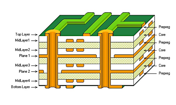
As the name suggests, a multilayer circuit board can only be called a multi-layer circuit board with more than two layers, such as four layers, six layers, eight layers, and so on. Of course, some designs are three-layer or five-layer circuit, also called multi-layer PCB circuit board.
Conductive wiring diagram larger than the two-layer board. The insulating substrate is separated between the layers. After each layer of the circuit is printed, each layer of the circuit is overlapped by pressing. After drilling, the electrical connection between them is usually achieved through plated through holes on the cross section of the circuit board.


Multilayer PCB or multilayer printed circuit boards are circuit boards composed of two or more conductive layers (copper layers). The copper layer is pressed together by the resin layer (prepreg). Due to the complexity of the multilayer PCB manufacturing process, low production volume, and difficulty in rework, their prices are relatively higher than a single layer and double-sided PCB.
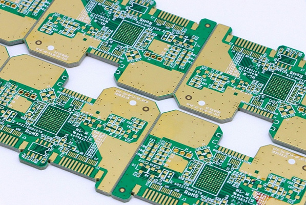
Ucreate manufacture multilayer PCB up to 56 Layer , accept pure single material or mixed-press materials :Fr4,Rogers,Polymide,metal Core . Send Your PCB Files to Sales@ucreatepcb.com, We will quote you Very Soon !

Due to the increase in the packaging density of integrated circuits, a high concentration of interconnection lines has resulted, which necessitates the use of multilayer PCB. Unforeseen design problems such as noise, stray capacitance, and crosstalk have appeared in the printed circuit layout. Therefore, the printed circuit board design must minimize the length of signal lines and avoid parallel routes. Obviously, in the PCB single-sided board, even the double-sided board, due to the limited number of crosses circuit that can be achieved, these requirements cannot be satisfied. In the case of a large number of interconnection and crossover requirements, the PCB circuit board must be expanded to more than two layers to achieve satisfactory performance. Thus a multilayer circuit board has appeared. Therefore, the original intention of manufacturing multilayer circuit boards is to provide more freedom in selecting appropriate wiring paths for complex and noise-sensitive electronic circuits.
Why are Multilayer PCBs Usually Widely Used?
- Multilayer PCBs are made utilizing high technology. This is why it is highly trusted due to the skills, processes, and designs required to manufacture it.
- You can also attribute it to the fact that users always want something modern.
- Its miniature size gives it its flexibility
- It has a small size, and its performance is enhanced with its technology. Most users prefer a device having a smaller size
- As a result of its less weight, it is portable enough and convenient for users. Users can easily carry the around, because they are not as bulky as some other smartphones.
- Due to its fabrication process, users consider this PCB as one with high quality
- It makes use of highly skilled professionals, modern technology, and high-quality materials.
- Easy installation, which makes it widely used, hence there is no need getting the service outsourced
Multilayer PCBs come with a protective layer, which prevents damage from coming to it, as well as an increase in its durability.
It is the most preferred due to its higher density, when compared to its counterparts. Users love devices that have a higher mass per volume degree, which should boast enough storage space.
Advantages and disadvantages of Fr-4 PCB
Advantages of Fr-4 PCB:
- Cost-effective: Fr-4 is an inexpensive material, making it an ideal choice for large-scale production runs.
- High thermal resistance: Fr-4 PCB can withstand high temperatures, making it suitable for applications that require high heat resistance.
- Excellent electrical insulation: Fr-4 PCB has excellent electrical insulation properties, making it suitable for applications that require high voltage.
- Good mechanical strength: Fr-4 PCB has good mechanical strength, making it suitable for applications that require high mechanical stress.
- Versatile: Fr-4 PCB can be used in a wide range of applications, from consumer electronics to aerospace and defense.
Disadvantage of Fr-4 PCB:
- Limited frequency range: Fr-4 PCB has limited frequency range, making it unsuitable for high-frequency applications.
- Limited chemical resistance: Fr-4 PCB is not resistant to certain chemicals, making it unsuitable for applications that require exposure to harsh chemicals.
Fr-4 PCB is used in a wide range of applications, including:
- Consumer electronics: Fr-4 PCB is used in consumer electronics such as smartphones, tablets, and computers.
- Industrial equipment: Fr-4 PCB is used in industrial equipment such as power supplies, motor controls, and automation systems.
- Aerospace and defense: Fr-4 PCB is used in aerospace and defense applications such as radar systems, satellite communication systems, and flight control systems.
- Medical equipment: Fr-4 PCB is used in medical equipment such as CT scanners, ultrasound machines, and defibrillators.
In conclusion, Fr-4 PCB is a widely used material for printed circuit boards due to its cost-effectiveness, durability, and versatility. It has excellent electrical insulation, high thermal resistance, and good mechanical strength. However, it has limited frequency range and chemical resistance. Fr-4 PCB is used in a wide range of applications, from consumer electronics to aerospace and defense, making it an important material in the electronics industry.
- Guarantee good service and quality from PCB quotation to delivery.

Deliver Time For PCB & PCBA
- PCB production time: sample: 3-4 days / production: within 7 days
- Fast pcb delivery: 24 hours for 2L ; 48 hours for 4L ; 72 hours for 6L.
- Component purchase: 2 days if all components is available in our domestic market.
- PCB Assembly: samples: within 8 days / mass production: within 12 days
|
LAYER |
PROTOTYPE |
MASS PRODUCTION (above 20 m2) |
|
|
Quick Turn |
Standard Time |
||
|
MC PCB |
48 hours |
4-5 days |
10-12 days |
|
PFC 1 L |
48 hours |
5-6 days |
12-13 days |
|
1L |
24 hours |
3-4 days |
8-10 days |
|
2L |
24 hours |
3-4 days |
8-10 days |
|
4L |
48 hours |
5-6 days |
8-10 days |
|
6L |
72 hours |
6-7 days |
10-12 days |
|
8L |
72 hours |
7-8 days |
12-14 days |
|
10L |
96 hours |
9-10days |
16-18 days |
|
PCB Prototype |
Quick Turn PCB |
Single-Sided PCB |
|
Double-Sided PCB |
Multilayer PCB |
|
|
Rigid-Flex PCB |
LED PCB |
|
|
Aluminum PCB |
Thick Copper PCB |
|
|
HDI PCB |
BGA PCB |
High TG PCB |
|
PCB Stencil |
Impedance Control PCB |
|
|
High-Frequency PCB |
Bluetooth Circuit Board |
Automotive PCB |
|
USB Circuit Board |
Halogen-Free PCB |
Antenna PCB |

