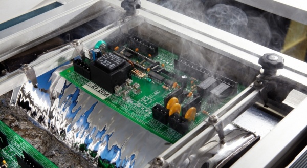
What is selective wave soldering?
Selective wave soldering, also known as robot soldering, is a special form of wave soldering invented to meet the development requirements of through-hole component soldering. Selective wave soldering generally consists of three modules: flux spraying, preheating and welding. Through the equipment programming device, the flux spraying module can complete the selective flux spraying on each solder point in turn. After preheating by the preheating module, the welding module completes the welding of each solder point point by point.
Advantages of selective wave soldering:
1.No special jigs or furnace trays are required during welding, which saves production costs.
2.Through-hole parts do not need to meet the high temperature resistance conditions of reflow soldering, but only meet the general wave soldering temperature conditions; circuit boards are not easily bent and deformed due to high temperatures.
3.Good welding quality and through-hole filling rate can be obtained during welding.
4.Save energy and cost, and do not require large tin furnaces, reflow furnaces and excessive tin bars like wave soldering.
5.The avoidance area is much smaller than the furnace tray for wave soldering.

Analysis and solutions of common defects of selective wave soldering:
1. Bridging: Bridging is a common defect in selective soldering. Bridging may be caused by too close spacing between component pins or unstable wave. The possible reasons are as follows: the welding temperature is set too low, the welding time is too short, the descending time is too fast after welding, and the amount of flux sprayed is too little. Generally, in this case, it is necessary to check the wave and confirm whether the welding coordinates are correct. It can be improved by increasing the welding temperature or preheating temperature, increasing the welding time, increasing the descending time, and increasing the amount of flux sprayed.
2. Tin overflow: In this case, it is generally necessary to check whether the through-hole components are missing, whether the board is obviously deformed, whether the furnace temperature setting is too high to cause PCB deformation, and secondly, check the matching between the component pin diameter and the through-hole diameter. If the through-hole is too large and the component pin is too thin, it will cause tin overflow. The wave height or welding height of the tin overflow part can be reduced, and the amount of flux sprayed can be reduced.
3. Tinning height cannot be reached: This is also a common defect for products above two. Generally speaking, some large metal components such as power modules are difficult to tin because they are mostly connected to the ground pins and dissipate heat quickly. Of course, the tinning height standard will be relaxed accordingly. In addition, low welding temperature, small amount of flux spraying, and low wave height will lead to insufficient tinning height. Increasing the preheating and welding temperature, spraying more flux, etc. can solve the problem.
4. Component lifting: If the component is too light or the wave is lifted, the wave will lift the component, or the component is not inserted in place when the component is inserted, and the track speed is too fast or unstable, causing the component to be tilted and lifted. A fixture can be made to hold the original part down. Due to the heat absorption of the fixture, the preheating or welding temperature may need to be increased.
5. Missing components: Check whether the missing components are on the wave soldering surface or the non-soldering surface. If the through-hole components are missing, the reason may be the same as the above component lifting. When the SMT components on the soldering surface are missing, pay attention to whether the soldering coordinates are set incorrectly during soldering, causing the wave to reach the components, and whether the wave is unstable and touches the nearby materials during soldering. In this case, the coordinates can be corrected or the materials near the through-holes can be protected with white glue, and the situation can be fed back to the DFM team.
6. Solder joint voids: If the component pins are too short to extend out of the through-holes or the cross-section of the component pins is oxidized and cannot be tinned, flux can be sprayed.
7. Tin pulling: This is a defect type with a higher frequency than bridging. Preheating and soldering temperatures are too low, and soldering time is too short to cause tin pulling.
8. Tin beads: If there are tin beads, check the quality of the flux or whether the surface of the board is stained with solder paste. The water in the flux will burst during soldering and cause tin beads.
9. Component pins become thinner and eat the pins: It may be that the welding temperature is too high or the welding time is too long, or the pin spacing is too close. When welding a pin, the wave band reaches the pin next to it, causing the pin to be welded twice. In this case, you can modify the coordinate parameters to avoid welding the pin twice. Pins that are too close can be welded.
10. Insufficient tin: The wave temperature is too low, the wave is unstable, the wave height or welding height is too low, and the welding coordinate setting is wrong, which will lead to insufficient tin. Correcting the coordinates, cleaning the tin nozzle, increasing the welding temperature, and increasing the wave or welding height can solve the problem.
The fundamental difference between wave soldering and ordinary wave soldering
Wave soldering is to contact the entire circuit board with the tin-spraying surface and rely on the surface tension of the solder to naturally climb to complete the soldering. For large heat capacity and multi-layer circuit boards, wave soldering is difficult to meet the tin penetration requirements. Ordinary wave soldering is suitable for mass production and does not require high-quality circuit boards.
If wave soldering is selected, only part of the soldering area is in contact with the solder, and the flux is only applied to the parts that need to be soldered. The dynamic tin wave that comes out of the welding nozzle directly affects the vertical tin penetration in the through hole; especially when performing lead-free soldering, because of its poor wettability, a more dynamic and strong tin wave is required. In addition, it is not easy to leave oxides on the wave with strong flow, which will also help improve the welding quality.
The soldering efficiency of selective wave soldering is indeed not as high as that of ordinary wave soldering, because selective soldering is mainly for high-precision PCB boards, which cannot be soldered by ordinary wave soldering. When traditional wave soldering cannot complete through-hole group soldering (defined in some special products, such as automotive electronics, aerospace, etc.), selective soldering with the help of programming to precisely control each solder joint is used. It is more stable than manual soldering and soldering robots, and the temperature, process, welding parameters, etc. are controllable and repeatable. It is suitable for products with increasingly miniaturized through-hole soldering and dense welds. Selective wave soldering has lower production efficiency than ordinary wave soldering (even for 24 hours), and the production and maintenance costs are high. The key to the solder joint yield depends on the NOZZLE state. Selective wave soldering is mainly for high-precision PCB boards and products that cannot be soldered by ordinary wave soldering. Selective wave soldering can be used for small-batch production, high requirements for welding quality, and limited site space.
Ucreate Electronic Group provides one-stop SMT patches, THT plug-ins, and finished product assembly and processing for various electronic products, providing the best quality products and services for your electronic product needs.
Related Posts:
1.Why is PCB solder mask necessary?
2.How Does Bad Conformal Coating Affect PCBA?
3.What is SMT patch wave soldering?
4.Top 10 PCB Circuit Board Manufacturers in China
5.What Are The Different Types of PCBs?
Welcome to consult our sales engineer with BOM list and Gerber file

