
Categories
Recent Posts
4. PCB processing prototype generated PCB processing file, you can transfer the file to the PCB processing factory, PCB processing prototype.
The PCB drawing method is now very much PCB drawing methods, common PCB drawing methods include the following:
1. Copper filling method is a simple and practical PCB drawing method, the operation is relatively simple for beginners to use. The basic principle is to pre-paint the PCB board with copper, and then use etching techniques to remove the unwanted parts can be.
2. Spacing (cut line) method spacing method is to make different component circuits relatively independent of a board, and then use small cards or pieces of paper attached to the board want to pin and lead the place for wire connection, the formation of PCB circuit.
3. The printing method printing method is to print the graphics on a printed film and chemically remove the copper skin covering the outside of the picture, you can get the circuit board drawing. This method of PCB production is more efficient, but it is more difficult to control the quality of the PCB board surface.
The PCB production process PCB production process is more complex, mainly including the following steps:
1. Pre-processing of the copper board for cleaning, degreasing and rough grinding steps, such as preparation of PCB substrate processing.
2. Photoresist PCB board surface in addition to the need to retain the part of the circuit, other places need to be photoresist. This process uses a UV light source to harden the photopolymer onto the PCB.
3. Image exposure and plastic etching The produced photoresist work is pressed together with Color Film and then placed in the exposure machine for exposure. After the exposure is complete, the board is etched and the next step is the etching process, where the part to be etched out is etched to create the PCB circuit.
4. Final processing after the completion of etching, the need for final processing, including the removal of UV light board adhesive, remove the solder slag on the line, polishing the line. After the final processing is completed, the complete PCB board can be obtained.
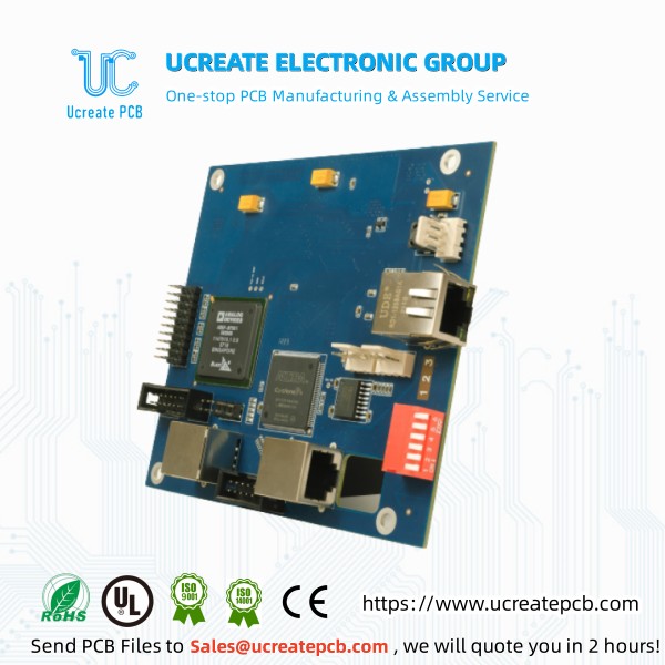
The PCB drawing process involves specifying the circuit board requirements, drawing out the circuit schematic and converting the schematic to a PCB processing file for final PCB processing and prototyping. The PCB process is also complex and requires pre-processing, photoresist, image exposure and plastic etching as well as final processing. Only with an in-depth understanding of the PCB drawing process and methods can we design a more perfect circuit board.
Send Your Inquiry to Sales@ucreatepcb.com, we will quote you in 2 hours!

Send your PCB Files or Bom List now
GET IN TOUCHE-mail : Sales@ucreatepcb.com
Office Address : Room 315, Building C, Yunhai Industrial Park, Longgang District, Shenzhen
PCB Factory :Xiangshui River Industrial Zone, Daya Bay, Huizhou. / No. 11, East District, Industrial Park, Suichuan County, Jiangxi Province
SMT Factory : 3/F, Building 28, Chentian Industrial Zone, Xixiang Street, Bao'an District, Shenzhen, China