Categories
Recent Posts
I. Why does PCB design require process edges and MARK points?
1. The role of process edge
The Fiducial Edge or Process Edge is a blank area reserved at the edge of the PCB, mainly used for:
• Production fixture positioning: SMT placement machines and other equipment need to fix the PCB through the process edge to ensure processing accuracy.
• Prevent damage to edge components: Avoid direct contact between the placement machine nozzle or conveyor belt and edge components to reduce the risk of damage.
• Ensure transmission stability: The process edge provides sufficient support to prevent the PCB from bending or shifting during transmission.
Design suggestions:
• The process edge width is usually ≥5mm (depending on equipment requirements).
• If the PCB size is small, the process edge can be increased through panelization.

2. The role of MARK point
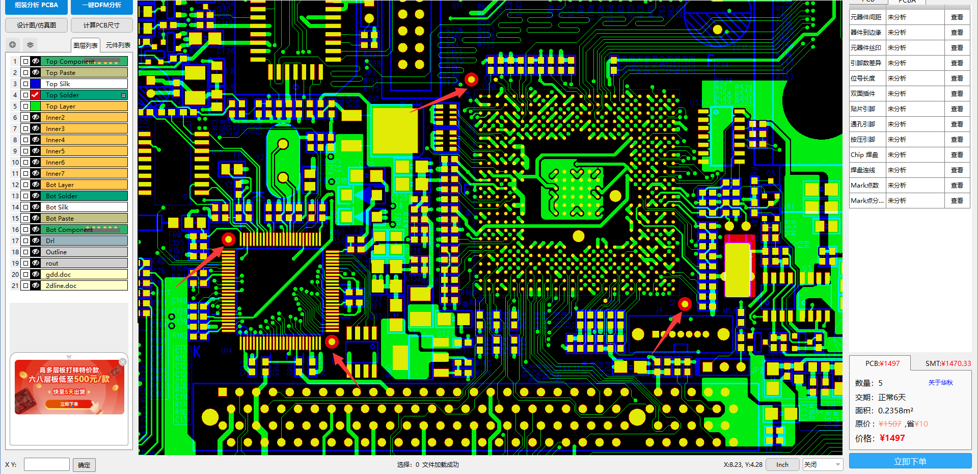
MARK point (reference point) is a special mark on the PCB, used for:
• SMT machine visual positioning: helps the equipment identify the PCB position and ensure accurate component placement.
• Improve placement accuracy: Especially in multi-panel or complex designs, MARK points can reduce alignment errors.
• Automated production calibration: The equipment adjusts the coordinate system through MARK points to ensure production consistency.
Design suggestions:
• It is usually necessary to place at least 1 MARK point on each diagonal of the PCB (2 to 4 in total).
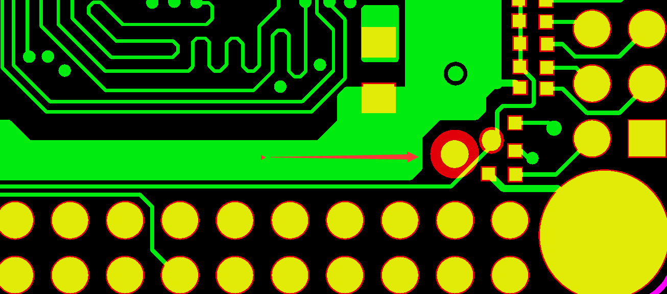
• The MARK point should be circular with a diameter of ≥1mm and a solder-free area of ≥3mm around it.
II. Method of adding process edge and MARK point
1. Adding process edges
• Single board design: Reserve a blank area of ≥5mm on the edge of the PCB (no components or traces are placed).
• Panel design: Multiple PCBs are divided by V-Cut or stamp holes, and the process edge needs to be retained on the outer edge of the panel.
• Design software operation (taking Altium Designer as an example):
Draw the process edge boundary line on the "Mechanical" layer.
Make sure there are no electrical components or traces in the process edge area.
2. Add MARK point
• Position selection: Usually located at the diagonal corner of the PCB (such as the upper left or lower right). If the panels are assembled, each sub-board needs a MARK point.
• Design Specifications:
• The MARK point should be a solid circle with an outer diamet
• There must be a ≥3mm solder-free area around it (to avoid solder coverage).
• Design software operation (taking Altium Designer as an example):
• Place a circular pad on the "Top Overlay" or "Bottom Overlay" layer.
• Set the pad attributes to "No Net" and adjust the size.

III. Conclusion
• Process edge: To ensure production stability and prevent edge damage, a blank area of ≥5mm needs to be reserved.
• MARK point: To improve the placement accuracy, it needs to be arranged diagonally to meet the diameter and spacing requirements.
• Design Tools: Easily added via dedicated layers in PCB design software, such as Mechanical or Overlay layers.
Reasonable design of process edges and MARK points can significantly improve PCB production efficiency and yield!
Welcome to consult our sales engineer with BOM list and Gerber file