Categories
Recent Posts
Designing PCBs and enclosures in parallel is the best way to ensure high-quality system designs. Learn how to use Fusion 360 to marry the 2D domain of PCB design with the 3D domain of mechanical enclosure design.
When designing a product that combines an electronic printed circuit board (PCB) with a mechanical enclosure, the interactions between all of the electronic parts, the circuit board, and the enclosure itself must be analyzed carefully.
This is often challenging because, in the electronics realm, the design process usually takes place in the 2D domain, where schematics and copper traces are created in parallel with the simple goal of guaranteeing electrical continuity. We extend this to the 3D domain by providing tools for modeling electronic components and parallelizing the enclosure's mechanical design such that it is always synchronized with the PCB.

An example is shown in Figure 1 where a USB Bluetooth accessory is designed across three domains in unison: mechanical, electrical, and electromechanical. The enclosure mates with the PCB using plastic pins for alignment, and the USB plug itself protrudes from the clamshell enclosure.
Multiple parts, including a complex Bluetooth module and several supporting passives, are modeled in 3D and connected electrically through the traces in the PCB. By simply switching environments in Fusion 360, the PCB and schematic can be depicted in the traditional 2D electrical domain.
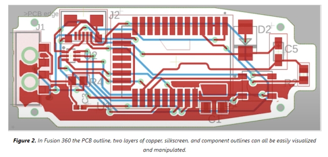
As shown in Figure 2, the PCB outline, two layers of copper, silkscreen, and component outlines can all be visualized and manipulated with ease. Changes to the schematic are immediately updated in the PCB layout, and changes in the PCB layout automatically propagate to the 3D electromechanical view.
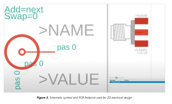
A common format for representing 3D CAD models is Standard for the Exchange of Product Data (STEP) files. Many manufacturers of electronic components offer these files for download and import into electrical CAD (ECAD) tools. As shown in Figure 3, the minimum requirement for ECAD design is to have a schematic representation (symbol) and a PCB representation (footprint).
Fusion 360 requires both in order to guarantee consistency between the PCB and the schematic, though it’s possible to assign multiple footprints to a single symbol to account for variants of a given part.
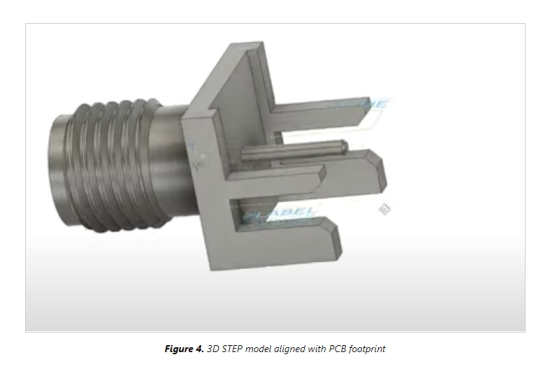
For 3D electromechanical integration, the STEP file must be downloaded and imported. The software platform allows this from within the component library, and requires only a few simple steps. Once the model is imported, it must be aligned to the footprint as shown in Figure 4.
Basically, each of the PCB pads must be tied physically to a feature on the 3D model. After this alignment is complete, the 3D part body will automatically appear within the top level electromechanical design.
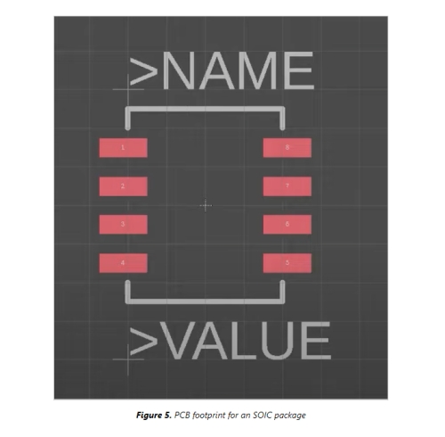
For example, a common 8-pin SOIC device footprint is shown in Figure 5. To generate an accurate 3D model of this part, the model generator can be invoked and its parameters adjusted to properly match the physical device.
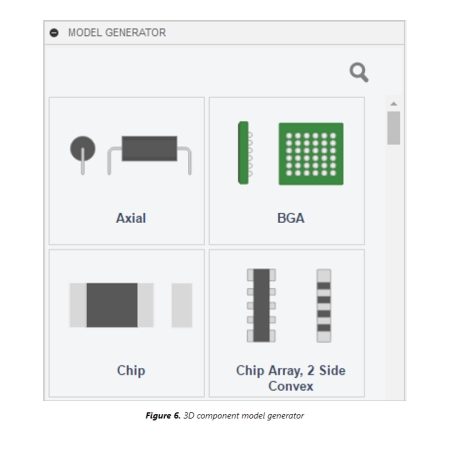
The model generator offers a wide variety of component families to choose from. As shown in Figure 6, a few examples include axial parts like through hole resistors, complex BGA ICs, surface mount passives, and surface mount chip arrays.
After selecting the SOIC family from the model generator, Fusion 360 presents a dialog of parameters ranging from basic items like pin count to complex IPC tolerances like placement and fabrication. The SOIC parameters are shown in Figure 7 and can be easily modified to match the 8-pin device under consideration.
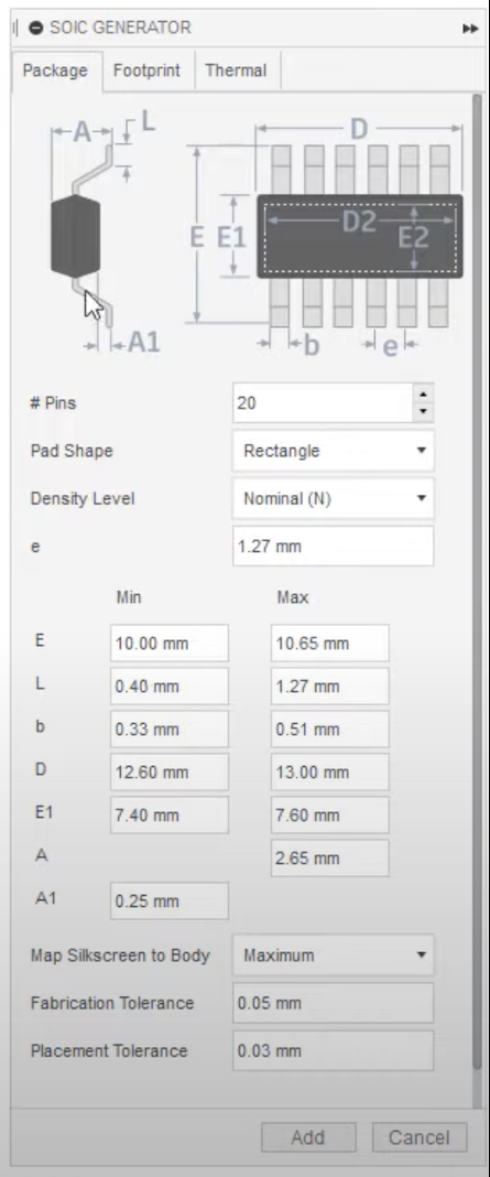
Once the appropriate values have been entered to match the physical device, Fusion 360 creates a functional 3D representation and a 2D footprint model based on standard electronics packaging techniques.
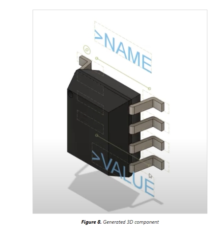
The 3D model and footprint are attached to the component within the library. As shown in Figure 8, the 8-pin SOIC chip looks like an exact match to the 3D physical device and can be used to validate electromechanical interference and form factor.
While there are many ways to tackle the issues of electromechanical integration, Fusion 360’s method links schematic symbols, PCB footprints, and 3D body models to a single point of truth in the component library. This enhances efficiency and reduces wasted design effort.
In addition, this software platform enhances this workflow by offering the ability to create 3D body models on the fly when manufacturer supplied data isn’t available. As a result, mechanical engineers, industrial designers, and electrical engineers can work in tandem to quickly create complex, high quality products.
Welcome to consult our sales engineer with BOM list and Gerber file