
Categories
Recent Posts
The Critical Art of Maximizing Power Transfer in High-Frequency Systems
In the ever-evolving landscape of wireless communications, the demand for higher data rates, broader bandwidths, and more efficient power delivery has pushed RF engineers to the frontiers of microwave and millimeter-wave (mmWave) frequencies. At these elevated frequencies—ranging from 1 GHz to well beyond 100 GHz—the design of RF power amplifiers (PAs) becomes increasingly complex, with impedance matching emerging as perhaps the most critical determinant of performance. This article explores the sophisticated impedance matching techniques that enable modern RF power amplifiers to deliver maximum power with minimal losses at microwave and mmWave frequencies.
Understanding the Fundamentals
Before diving into advanced matching techniques, it's essential to grasp why impedance matching is so crucial in RF power amplifier design. At its core, impedance matching ensures maximum power transfer from the source to the load while minimizing reflections that can cause signal distortion, power loss, and potential damage to sensitive components.
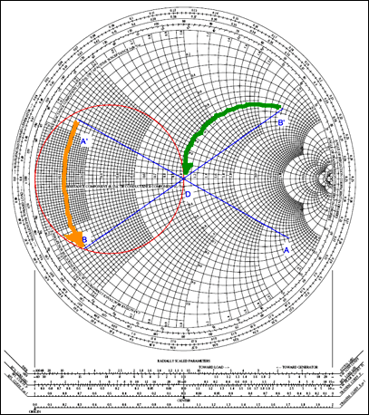
(Figure 1: The Smith Chart remains an indispensable tool for visualizing impedance transformations in RF design.)
The fundamental principle stems from the maximum power transfer theorem, which states that maximum power is delivered when the load impedance equals the complex conjugate of the source impedance. In practical PA design, this means transforming the typically low impedance of power transistors (often just a few ohms) to the standard system impedance of 50 ohms used in most RF systems.
At microwave frequencies, wavelength effects become significant. Transmission lines no longer behave as simple conductors but as distributed elements where voltage and current vary along their length. This distributed nature necessitates careful consideration of line lengths, characteristic impedances, and termination conditions.
The Challenge of mmWave Frequencies
As we push into mmWave territory—frequencies above 30 GHz where wavelengths shrink to millimeters—the challenges multiply exponentially. Parasitic elements that were negligible at lower frequencies now dominate circuit behavior. Bond wires, package leads, and even PCB trace geometries introduce significant inductance and capacitance that can completely alter the impedance characteristics of a circuit.
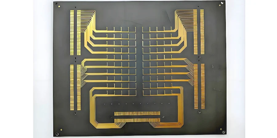
(Figure 2: High-frequency mmWave antenna array PCBs demonstrate the intricate routing required for 5G/6G communication systems.)
At these frequencies, the active device impedance becomes highly frequency-dependent and often exhibits significant variation across the operating bandwidth. The output impedance of a GaN or GaAs power transistor at 28 GHz, for instance, may have a real part of only 2-5 ohms with a substantial reactive component that varies rapidly with frequency. This presents a formidable matching challenge, particularly when wide bandwidth operation is required for modern communication standards like 5G NR or Wi-Fi 6E/7.
Classical Matching Network Topologies
L-Section Networks
The simplest form of impedance matching employs L-section networks, consisting of two reactive elements arranged in either a low-pass or high-pass configuration. These networks are particularly effective for narrowband applications where the load impedance remains relatively constant across the frequency range of interest.
The design procedure involves calculating the required series and shunt reactances to transform the load impedance to the desired source impedance. While mathematically straightforward, L-section networks suffer from limited bandwidth and are rarely used alone in modern wideband PA designs.
Pi and T Networks
For applications requiring greater bandwidth or higher impedance transformation ratios, Pi and T networks offer more flexibility. These three-element networks can be designed to achieve specific quality factor (Q) values, allowing engineers to trade off bandwidth against matching network complexity and loss.
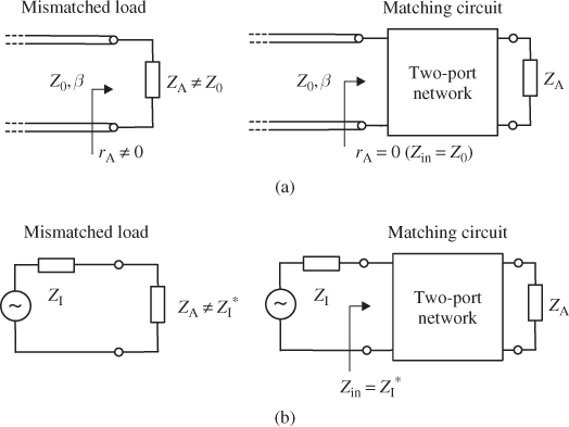
(Figure 3: Basic impedance matching configurations showing mismatched loads and their corresponding matching circuits.)
At microwave frequencies, these lumped-element networks face practical limitations. As frequencies increase, the required inductor and capacitor values become impractically small, and the parasitic effects of real components begin to dominate. This leads us to distributed matching techniques that are essential for mmWave applications.
Distributed Matching Techniques
Quarter-Wave Transformers
One of the most elegant solutions in microwave engineering is the quarter-wave transformer. By inserting a transmission line segment of length λ/4 with characteristic impedance Z₁ = √(Z₀ × Z_L) between the source (Z₀) and load (Z_L), perfect impedance matching is achieved at the design frequency.
However, the quarter-wave transformer is inherently narrowband. To achieve broader bandwidth, multiple quarter-wave sections can be cascaded, creating a multisection transformer with Chebyshev or binomial response characteristics. These designs can achieve octave or greater bandwidths while maintaining excellent return loss.
Microstrip and Stripline Implementation
At microwave and mmWave frequencies, transmission line matching networks are typically implemented using microstrip or stripline technologies. Microstrip lines, consisting of a conductor strip on a dielectric substrate with a ground plane beneath, offer ease of fabrication and integration with planar circuits.
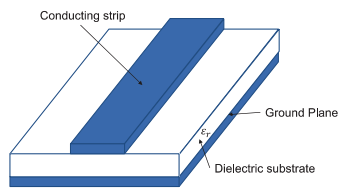
(Figure 4: Microstrip transmission line structure showing the conducting strip, dielectric substrate, and ground plane configuration.)
The characteristic impedance of microstrip lines depends on the strip width, substrate thickness, and dielectric constant. By tapering line widths or using stepped-impedance sections, smooth impedance transitions can be realized. At mmWave frequencies, substrate selection becomes critical—low-loss materials like Rogers RO4350B, Taconic TLY-5, or advanced ceramics are preferred to minimize insertion loss in matching networks.
Advanced Matching Techniques for Power Amplifiers
Load Pull and Source Pull Techniques
Modern PA design relies heavily on load pull and source pull characterization to determine the optimal impedance conditions for maximum output power, efficiency, or linearity. These measurement techniques systematically vary the load impedance presented to the device under test while monitoring performance parameters.
The results are typically plotted on a Smith Chart, creating contours of constant power, efficiency, or gain. The optimal load impedance for maximum power delivery rarely coincides with the conjugate match condition—power amplifiers are often designed to present a specific "load line" impedance that maximizes voltage and current swing within the device's safe operating area.
(Figure 5: Fundamental concept of impedance matching networks connecting transmission lines to arbitrary loads.)
Broadband Matching Strategies
For wideband power amplifiers covering multiple octaves, conventional matching techniques prove insufficient. Several advanced approaches have been developed:
Non-Foster Matching:By using active circuits to create negative impedance elements, non-Foster networks can achieve broader bandwidth than passive networks alone. These techniques are particularly valuable for electrically small antennas and ultra-wideband applications.
Real Frequency Technique (RFT):Developed by H.J. Carlin, the Real Frequency Technique designs matching networks directly from measured or simulated impedance data without requiring a circuit model. This data-driven approach is invaluable for wideband PA design where simple circuit models fail to capture device behavior.
Simplified Real Frequency Technique (SRFT):An extension of RFT that provides closed-form solutions for certain network topologies, making it more practical for routine design work while maintaining the benefits of direct impedance synthesis.
Harmonic Tuning and Waveform Engineering
High-efficiency PA modes (Class E, F, J, etc.) rely on precise control of harmonic impedances in addition to the fundamental frequency match. Harmonic tuning networks present specific impedances at the second, third, and sometimes higher harmonics to shape the voltage and current waveforms at the device output.
At microwave frequencies, achieving the required harmonic terminations while maintaining fundamental matching requires sophisticated multi-harmonic matching networks. These often employ stepped-impedance lines, open/short stubs, or coupled-line structures to create frequency-selective impedance characteristics.
mmWave-Specific Considerations
Electromagnetic Coupling and Parasitics
At mmWave frequencies, electromagnetic coupling between adjacent structures becomes a significant concern. Matching network elements must be carefully laid out to minimize unintended coupling that could alter impedance characteristics. Electromagnetic simulation tools (ANSYS HFSS, Keysight EMPro, CST Microwave Studio) are essential for verifying matching network performance before fabrication.
Package and Bond Wire Effects
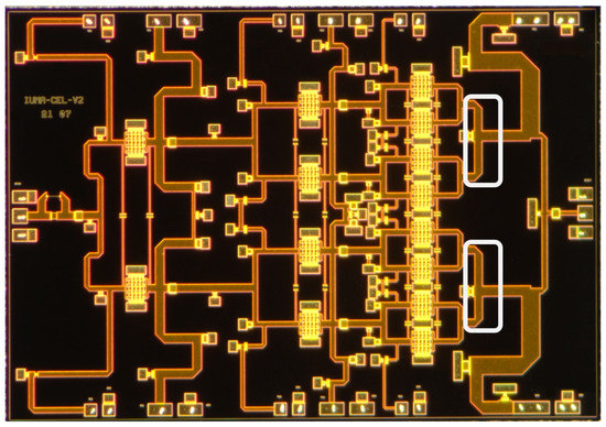
The transition from the semiconductor die to the external circuit introduces substantial parasitic elements. Bond wires add series inductance (typically 0.5-1 nH per millimeter), while package leads contribute both inductance and capacitance. At 60 GHz, even 0.5 nH of inductance presents a reactance of nearly 190 ohms—enough to completely destroy impedance matching.
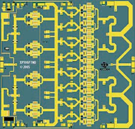
(Figure 6: GaAs MMIC high-power amplifier chip showing intricate transmission line networks and power combining structures.)
Modern mmWave PAs increasingly employ flip-chip or wafer-level packaging to minimize these parasitic effects. In these configurations, matching networks can be partially or fully integrated on the semiconductor die itself, eliminating bond wire inductance and enabling more precise impedance control.
Integrated Matching Networks
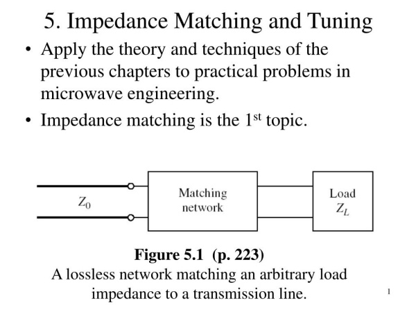
Monolithic Microwave Integrated Circuits (MMICs) allow for the integration of matching networks directly on the semiconductor substrate. This approach offers several advantages at mmWave frequencies:
(Figure 7: Ku-Band GaN-on-Si MMIC power amplifier die photograph showing integrated matching networks and power combining architecture.)
Emerging Technologies and Future Directions
Artificial Intelligence in Matching Network Design
Machine learning algorithms are increasingly being applied to impedance matching network synthesis. Neural networks trained on extensive electromagnetic simulation databases can rapidly propose matching topologies that would require hours of manual optimization. These AI-driven approaches are particularly valuable for multi-objective optimization where power, efficiency, bandwidth, and linearity must be simultaneously balanced.
Reconfigurable and Tunable Matching
Future 5G and 6G systems will require PAs capable of operating across widely separated frequency bands. Tunable matching networks using MEMS switches, varactor diodes, or ferroelectric materials enable dynamic impedance adjustment to maintain optimal performance across multiple bands. While these techniques add complexity, they offer a path to true multi-band, multi-standard power amplifiers.
3D Integration and Advanced Packaging
Three-dimensional integration technologies, including through-silicon vias (TSVs) and embedded die packaging, are opening new possibilities for mmWave matching networks. By distributing matching elements in multiple layers, higher quality factors and more compact implementations become possible. These advanced packaging approaches will be essential as carrier frequencies push toward the sub-THz range for future 6G systems.
Conclusion
Impedance matching for RF power amplifiers at microwave and mmWave frequencies represents a sophisticated discipline that bridges classical transmission line theory with cutting-edge semiconductor technology. As wireless systems demand ever-higher frequencies and bandwidths, the challenges of efficient power transfer only intensify.
The successful PA designer must master a diverse toolkit: from Smith Chart manipulations and distributed matching theory to electromagnetic simulation and advanced characterization techniques. The transition from lumped elements to distributed networks, the management of parasitic elements, and the integration of matching functions onto semiconductor dies all represent critical capabilities for modern RF engineering.
Looking ahead, the continued evolution of 5G, the emergence of 6G, and the proliferation of radar and sensing applications at mmWave frequencies will drive further innovation in impedance matching techniques. Whether through AI-assisted design, tunable networks, or novel integration technologies, the quest for perfect impedance transformation remains at the heart of RF power amplifier excellence.
For engineers entering this field, the message is clear: impedance matching is not merely a design step—it is the foundation upon which all high-frequency power amplifier performance is built. Mastering these techniques is essential for anyone seeking to push the boundaries of wireless communication technology.
Send your PCB Files or Bom List now
GET IN TOUCHE-mail : Sales@ucreatepcb.com
Office Address : Room 315, Building C, Yunhai Industrial Park, Longgang District, Shenzhen
PCB Factory :Xiangshui River Industrial Zone, Daya Bay, Huizhou. / No. 11, East District, Industrial Park, Suichuan County, Jiangxi Province
SMT Factory : 3/F, Building 28, Chentian Industrial Zone, Xixiang Street, Bao'an District, Shenzhen, China