
Categories
Recent Posts
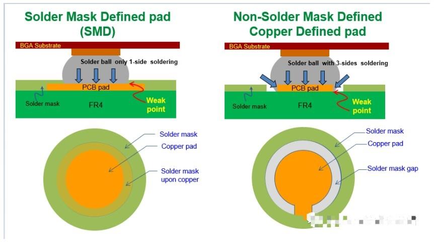
Proper PCB pad design is critical for efficiently soldering components to the board. For bare pad assembly, there are two common soldering methods - Soldermask Definition (SMD) and Non-Soldermask Definition (NSMD), each with its own features and advantages.
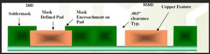
SMD (Solder Mask Defined Pad) is a pad size defined by the soldermask, and the pad size is determined by the green oil process.
NSMD (Non-Solder Mask Defined Pad (Copper Defind Pad)) pad size is defined by the pad, the pad size is determined by the etching process, that is, the opening window will be larger than the pad, our general design is this way.
Difference between SMD and NSMD:
Advantages and Disadvantages of SMD and NSMD
SMD advantages:
1, SMD pad moulding shape regular, not subject to the influence of the alignment, suitable for small parts pads, such as 0402, 0201, 01005
2, SMD pad maintenance is not easy to tear and fall off, because the actual size of the SMD pad copper foil relative to the NSMD to come to a large, and green oil covers part of the pad, so the pad and the substrate of the bonding strength is relatively good.
SMD disadvantages:
1, SMD because the green oil cover to the pad, resulting in the stencil than NSMD to be higher than the thickness of a green oil, increasing the amount of tin, the production process is more likely to cause a short-circuit, need to pay special attention to this point.
2, reduces the copper surface area available for solder joints and reduces the space between adjacent pads. This limits the width of the alignment between the pads, and may affect the use of through-holes, PCB Layout alignment will be more difficult;
3, SMD pads will be relatively poor solder strength. This is because its relative tin eating area becomes smaller, and SMD pads around the pressure of the green oil, green oil in the flow through the soldering high temperature thermal expansion and contraction occurs, but also affects the junction of the solder and green paint tin eating effect.
NSMD advantages:
1, NSMD tin eating area is relatively large, NSMD solder strength is higher than SMD
2, The gap between the pads is larger (compared with SMD), allowing a wider line width and more flexibility of the through-hole, PCB Layout will be easier to route!
NSMD disadvantages:
1, NSMD pad shape is affected by the alignment, there may be a different pad area at both ends of the same chip. It is easy to find the phenomenon of monumental personal recommendations, soft board design with SMD pad design, hard board design of small parts (size less than 0402 parts) with SMD design, the other with NSMD design, because the NSMD design is relatively simple.BGA with a mix of mounting, function of the PIN with SMD design, fixed PIN with NSMD design!
2, NSMD is an isolated pad, relatively easy to fall off in the maintenance process.
Ucreate PCB engineer, soft board design with SMD pad design, hard board design small parts (size less than 0402 parts) with SMD design, the other with NSMD design, because the NSMD design is relatively simple.BGA with mixed mounting, functional PIN with SMD design, fixed PIN with NSMD design.
Related Posts:
1.Why is PCB solder mask necessary?
2.What Are The Different Types of PCBs?
4.How much temperature can the PCB withstand?
5.Three Different Ways to Make a Blind Via Hole
Welcome to consult our sales engineer with BOM list and Gerber file
Send your PCB Files or Bom List now
GET IN TOUCHE-mail : Sales@ucreatepcb.com
Office Address : Room 315, Building C, Yunhai Industrial Park, Longgang District, Shenzhen
PCB Factory :Xiangshui River Industrial Zone, Daya Bay, Huizhou. / No. 11, East District, Industrial Park, Suichuan County, Jiangxi Province
SMT Factory : 3/F, Building 28, Chentian Industrial Zone, Xixiang Street, Bao'an District, Shenzhen, China