
Categories
Recent Posts
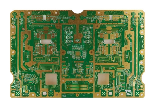
PCB circuit boards are all around us in every gadget we use. Be it the smart phone or a simple calculator; their function depends on the performance of PCBs.
Do you know what is a PCB?
The material encompassed by the printed circuit board includes:
• Copper: the copper gathers on the thick layer of foundation known as the substrate. Depending on the type of board and use, there can be one or two copper layers present.
The copper layer can exist on one side of the PCB, or it may be present on both sides of the substrate. Simple electronic devices make use of PCBs, which have a copper layer only on one side.
Copper layers are much thinner and delicate than the substrate.
The copper used in PCBs is referred to by weight and presented in ounces per square foot. Most common PCBs come with a copper content of 1 ounce of copper per square foot.
While the amount of copper present in the circuit board determines the amount of power, it will exchange.
• Silkscreen: the silkscreen performs the responsibility of making the printed circuit board readable to technology programmers by adding numerical and letter indicators.
• Substrate: the substrate is commonly known as FR4, which is an acronym for Fire Retardant.
It functions in providing a thick layer of foundation for the printed circuit board, which, of course, varies. However, you will find their thickness to change. It is the layer that offers rigidity to the PCBs.
It can also be made from flexible materials, which sometimes can be stretched too. Recently many innovative materials are being used to create the substrate, some of which are even plant-based.
Why use flexible circuit boards?
Creating a custom Printed Circuit Board (PCB) involves several steps, from initial design to fabrication and assembly. Here's a step-by-step guide to help you create a custom PCB:
1. Define Your Project:
Clearly define the purpose and requirements of your PCB project.
Identify the components, connectors, and features your PCB needs.
2. Schematic Design:
Create a schematic diagram of your circuit using PCB design software.
Choose symbols for components and connect them with wires to define the electrical connections.
Here are some PCB design software list:
PCB Artist
Ultiboard
Altium Designer 17
SOLIDWORKS PCB
DipTrace
PCBWeb
BSch3V
XCircuit
Gerbv
KiCad EDA
DesignSpark PCB
Eagle PCBs
CircuitMaker
Pad2pad
OrCAD
ZenitPCB
CircuitStudio
PCB123
AUSPICE
FreePCB

3. Component Selection:
Choose the components you'll use in your circuit based on the schematic.
Pay attention to specifications like voltage, current, package type, and availability.
Here is the guide for What are the components of PCBs?
4. PCB Layout:
Transfer your schematic to the PCB layout design view in the software.
Place components on the PCB, considering factors like component orientation, heat dissipation, and signal paths.
Route traces to connect components according to your schematic.
Pay attention to signal integrity, power distribution, and thermal management.
PCB layout tutorial:
It is the first step associated with the PCB tutorial. After you have successfully done your schematics, you can convert into PCB by clicking on "convert to PCB" on the editor that you are making use of.
The second step is to place the document exactly where you want to be positioned. If you are the type that prefers a clean-looking printed circuit board, components with similar functions should be placed side by side.
The first thing to do is go to the layer menu, click on the board outline layer, click on the current outline, and delete it after completing a new system with the PCB tools.
The copper area is the best thought of when many parts are joined to just a signal. This copper area can be created using the tools menu.
Depending on the type of current, there are two approaches to this method. If you have a low current creating the printed circuit board, the auto-router function can be used. If there is a need for different track sizes, it would be better if you did this manually. The auto-router function can be found at the top of the page.
Of course, you might need to mount your printed circuit board on something; in so doing, holes are required. The Hole tool can be found on the Tools menu, and then locate the spot you want.
Do you know How to drill holes in thick copper pcb?
In doing this, you would need to stroll to the tools menu and locate either the image or text tool. You can position the text as you wish and change the required layer or the book itself.
After completing the above steps, you can round up your work by viewing the result. You can change the color or some other features. Once you are ok with the product, click on "fabrication output" to buy the PCB.
5. PCB Design Rules:
Set up design rules in your PCB design software to ensure proper trace widths, clearances, and other design constraints.
Verify your design against these rules to avoid common errors.
6. Ground Plane and Power Planes:
Use ground and power planes for better signal integrity and noise reduction.
Connect all ground and power pins to these planes.
7. PCB Design Considerations:
Add silkscreen markings, reference designators, and any necessary labels.
Include mounting holes and connectors.
Pay attention to the mechanical aspects of your PCB, ensuring it fits within your enclosure or project.
8. Design Verification:
Perform a design rule check (DRC) and electrical rule check (ERC) using your PCB design software.
Review your design carefully for errors and signal integrity issues.
9. Generate Gerber Files:
Gerber files are industry-standard files used for PCB manufacturing.
Export Gerber files from your PCB design software, including layers for copper traces, solder mask, and silkscreen.

10. Choose a PCB Manufacturer:
Research and select a PCB manufacturer or fabrication service.
Provide them with your Gerber files and specify your PCB's material, thickness, and other requirements.
UcreatePCB is one of he leading PCB&PCBA manufacturer in China, manufacture according to your Design-BOM,Gerber file and testing procedures,while providing you best recommendations for easy manufactuing and cost saving.
Here is the guide for you to choose the right PCB supplier:
Not Sure If Your PCB Design Is Manufacturable?
11. Review Manufacturing Files:
Review the manufacturer's design guidelines to ensure your design complies with their capabilities.
Double-check your Gerber files for accuracy.
12. PCB Fabrication:
Place an order with the PCB manufacturer.
They will manufacture your custom PCB based on your design and specifications.
13. PCB Assembly:
Once you receive the fabricated PCBs, you can assemble them.
Solder the components onto the PCB using the appropriate techniques, whether by hand or through automated assembly.
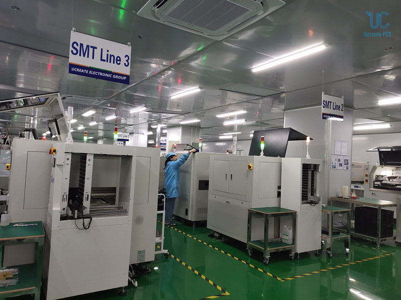
Ucreate Electronic Group has own STM Factory, 5 automatic SMT lines, advanced Hitach screen printer, Fuji NXT-ii SMT machines, Fuji XPF-L module SMT machines, X-Ray machine, BGA inspection. Can produce 10000 SQM/month, all products comply with ISO, RoHs , UL, IATF.
14. Testing and Debugging:
Power up the assembled PCB and test its functionality.
Debug and troubleshoot any issues that may arise.
15. Documentation:
Create comprehensive documentation for your custom PCB, including a bill of materials (BOM), assembly instructions, and schematics.
This documentation is essential for future reference and for scaling production if needed.
Ucreate is a professional electronic contract manufacturing factory,
You can send you Gerber files or BOM list to us for free quotation.
16. Compliance and Certification (if applicable):
Ensure your PCB meets any necessary regulatory or safety standards.
Obtain certifications if required for your application.
UcreatePCB can produce 10000 SQM/month, all products comply with ISO, RoHs , UL,CE IATF. We fabricate high quality for Class 2 and Class 3 PCBs.
The Difference Between Class 2 and Class 3 in the PCB IPC Standards.
17. Scaling Production (if applicable):
If your custom PCB is for commercial purposes, plan for mass production and consider cost optimization.
Creating a custom PCB requires careful planning, attention to detail, and a good understanding of electronics and PCB design principles. Be prepared for multiple design iterations and testing phases to ensure a successful outcome. Additionally, seek guidance and support from experienced PCB designers or engineers if needed.

Welcome to consult our sales engineer with BOM list and Gerber file
Send your PCB Files or Bom List now
GET IN TOUCHE-mail : Sales@ucreatepcb.com
Office Address : Room 315, Building C, Yunhai Industrial Park, Longgang District, Shenzhen
PCB Factory :Xiangshui River Industrial Zone, Daya Bay, Huizhou. / No. 11, East District, Industrial Park, Suichuan County, Jiangxi Province
SMT Factory : 3/F, Building 28, Chentian Industrial Zone, Xixiang Street, Bao'an District, Shenzhen, China