Categories
Recent Posts
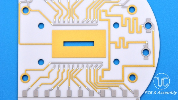
Ceramic PCBs are made by bonding copper foil directly onto the surface (single or double-sided) of a ceramic substrate such as aluminium oxide (Al₂O₃;) or aluminium nitride (AIN) at high temperature. This special process gives the ceramic PCB excellent electrical insulation properties, high thermal conductivity characteristics, excellent soft brazing properties and high adhesion strength.
The process of ceramic PCB board production is mainly divided into the following steps:
1. Design the circuit diagram
First, you need to use circuit design software to design according to the circuit design requirements. When designing, you need to consider factors such as circuit layout, branches, power consumption, etc. to ensure the stability and reliability of the circuit. After the design is completed, the circuit diagram needs to be exported to the Gerber file format for use in the subsequent board making process.
2. Making a substrate
Making a substrate is a key step in making a ceramic PCB. First, you need to select high-purity ceramic powder, and then make it into a ceramic substrate through selection, mixing, pressing and other processes. Then, drilling and copper foil covering are performed on the substrate to form the basic form of the conductive path and the circuit board.
3. Make graphics
Based on the Gerber file exported from the circuit diagram, use photolithography technology to make circuit graphics on copper foil. This process requires the use of a laser lithography machine to transfer the information of the Gerber file to the copper clad board to form a circuit graphic. The advantages of photolithography technology are high precision and high speed, which can meet the production requirements of high-density circuit boards.
4. Metallization treatment
Metallization treatment is the process of converting the copper foil on the circuit pattern into a conductive wire. This process requires a layer of metal to be plated on the surface of the copper foil, usually using a nickel-gold process. The purpose of metallization treatment is to protect the circuit pattern and improve the conductivity and corrosion resistance.
5. Applying enamel
The purpose of applying enamel is to protect the circuit board and improve the insulation performance. The enamel is a coating made of a mixture of ceramic powder and glass powder, which has the characteristics of high temperature resistance, corrosion resistance, and high insulation performance. The enamel needs to be applied by spraying, brushing, etc., and then sintered at high temperature to form a hard and dense ceramic protective layer.
6. Punching and plug-in
After the coating is completed, drilling and plug-in operations are required. Punching is to connect circuits of different layers, and plug-in is to connect circuit boards and other components. This process requires the use of drilling machines, placement machines and other equipment to complete.
7. Testing
Finally, the manufactured ceramic PCB board needs to be tested to ensure the correctness and stability of the circuit. The testing methods include electrical testing, insulation testing, environmental adaptability testing, etc.
The production process of ceramic PCB requires careful processing in multiple links, and the quality of each link will directly affect the performance and reliability of the circuit board. Therefore, every detail needs to be strictly controlled during the production process to ensure the production of high-quality ceramic PCB boards.

Ucreate PCB factory can not only make ceramic boards, but also fr4 boards, metal boards, transparent boards, soft boards, hard-soft boards, including single-layer, double-layer, multi-layer and other high-difficulty, high-frequency and high-speed boards. Our factory can produce up to 200,000 SQM per month. Friends with PCB & PCBA needs around the world are welcome to send us Gerber files at any time. Our professional sales engineers and technical engineers will give you free quotes within 4 hours.
Ceramic PCB Features and Advantages
1. Excellent electrical insulation performance: Ceramic materials themselves have extremely high resistivity, so ceramic PCBs perform well in electrical performance and can withstand high voltage and high current.
2. High thermal conductivity: Ceramic materials such as alumina and aluminum nitride have good thermal conductivity, which allows ceramic PCBs to dissipate heat effectively, especially for high-power power electronic circuits.
3. Excellent solderability and high adhesion strength: The surface treatment process of ceramic PCBs makes the bonding between copper foil and ceramic substrate very strong, and can withstand large mechanical and thermal stresses.
4. Etchability: Ceramic PCBs can be etched like ordinary PCBs to produce various complex circuit patterns.
5. Large current carrying capacity: Since ceramic PCBs have excellent electrical insulation and high thermal conductivity, they can withstand large currents without heating or damage.
Application Areas
1. High-power power electronic circuits: The high thermal conductivity and excellent electrical insulation properties of ceramic PCB make it the basic material for high-power power electronic circuit structure technology and interconnection technology.
2. Medical devices: Ceramic PCB is used in the electronic control systems of various medical devices, such as surgical instruments, therapeutic instruments, etc.
3. Communication systems: In mobile communication base stations, satellite communication equipment, radar and other communication systems, ceramic PCB is used in key parts such as signal processing and power amplification.
4. Home appliances: In the manufacture of home appliances such as televisions, audio equipment, and game consoles, ceramic PCB is used in key parts such as signal processing, power management, and control circuits.
5. Digital products: Ceramic PCB is also used in the manufacture of various digital products, such as mobile phones, tablet computers, and laptops, for key parts such as signal processing and control circuits.
Related Posts:
1. What is a rigid-flex board?
3.Why use flexible circuit boards?
4.Why is PCB solder mask necessary?
5.Top 10 PCB Circuit Board Manufacturers in China
Welcome to consult our sales engineer with BOM list and Gerber file